Tungsten Selenide

Introduction
Name: Tungsten SelenideOther name: Tungsten(Iv) Selenide
CAS:12067-46-8
Fórmula: 2Se2W
olecular Weight:343.77600
Exact Mass:345.80000
Nature
The thermal conductivity of tungsten diselenide (WSe2) is about hundred thousandth of the best thermal conductivity diamond, and being the world's lowest thermal conductivity material. In general, the worst thermal conductivity material (or known as a thermal insulator) is the so-called porous material.
Heat transfers in the crystal in the state of phonon. So if the crystal structure is quite predictable, then phonons can easily spread to distant, that is to say the material has a high thermal conductivity. Conversely, if the regularity of the atoms of the lattice structure is poor, phonon lattice energy will soon be consumed, and then the thermal conductivity would be very poor.
David Johnson (David c.Johnson), a chemistry professor in University of Oregon in US had found that, the thermal conductivity of tungsten diselenide thin-film is worse than monocrystalline tungsten diselenide, probably only hundred thousandth of the best thermal conductivity diamond. This new material has not only thermal conductivity like porous material, but also has high density which is probably the same to copper.
Use
The low thermal conductivity of tungsten diselenide means heat dissipation is not easy in the system, in other words, the energy conversion efficiency of the system will be higher. Therefore, the application of this new material will likely dramatically improve the efficiency of energy use.
Researchers in Vienna University of Technology in Austria first developed a diode made by a tungsten diselenide (WSe2), and the experiments showed that this material may be used for thin flexible solar cell.
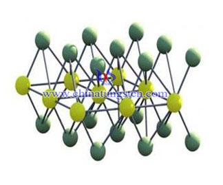
The main structure of tungsten diselenide (WSe2) is the upper and lower layer selenium atoms are connected by tungsten atoms in the intermediate layer. WSe2 can absorb light just like the graphene, and the light absorbed can used to generate electricity.
The thin layer is indeed light and thin which can permit about 95% of the light passing through, but the remaining one-tenth of 5% of the light will be absorbed by the material and converted into electricity. Therefore, its internal efficiency is very high. If multiple thin layers stacked on each other, a large part of this incident light ray can be effectively utilized, however this high transparency may sometimes bring beneficial side effects.

